
What is synchronous? Describe synchronous sequential circuits [Bangladesh Water Development Board -2018]
Classification Of Sequential Circuits
Sequential
circuits fall into two classes: synchronous and asynchronous.

·
Synchronous circuits:
In synchronous circuits the input
are pulses (or levels and pulses) with certain restrictions on pulse width and
circuit propagation delay. Therefore synchronous circuits can be divided
into clocked sequential circuits and uncklocked
or pulsed sequential circuits.
In a clocked sequential circuit which has flip-flops or, in some instances, gated latches, for its memory elements there is a (synchronizing) periodic clock connected to the clock inputs of all the memory elements of the circuit, to synchronize all internal changes of state.
Hence the operation of the entire circuit is controlled and synchronized by the periodic pulses of the clock.

On the other hand in an unclocked or pulsed sequential circuit, such a clock is not present. Pulse mode circuits require two consecutive transitions between 0 and 1 - that is a 0-pulseor a 1 pulse to alter the circuit’s state. A pulse -mode circuit is designed to respond to pulses of certain duration; the constant signals between the pulses are “null” or “spacer” signals, which do not affect the circuit’s behavior

From the above block diagrams we can note the following:
1) Pulse
outputs: For pulsed sequential circuits these occur only for the duration
of the respective input pulse and in some cases for duration considerably less.
For clocked sequential circuits these outputs occur for the duration of the
clock pulse.
2) Level
outputs: These change state at the start of the respective input or clock
pulse and remain in that state until the next state of output is required.
A requirement of synchronous sequential circuits is that the duration of the activating pulse or clock pulse should be sufficiently low in value that the pulse (or clock) has disappeared by the time the secondaries (the flip-flops outputs) have taken on their new value; otherwise the circuit will change state again. This means that the storage elements (flip-flops) should be edge-triggered devices (for example: D-type flip-flop, the JK flip-flop and their derivatives).
Analysis of Synchronous Sequential Circuits
As mentioned earlier, a sequential circuit contains one or
more flip flops and may or may not include logic gates. The circuits in Figure
8.20 are both sequential circuits.

Difference between battery &capacitor [Bangladesh Bank assistant Maintenance Engineer-2017]
Comparison between Capacitor and Battery:
|
Capacitor |
Battery |
|
In
capacitors, energy is stored in their electric field. |
Battery
is a device that consists of electrochemical cells that convert stored
chemical energy into electrical energy. |
|
·
High
Voltage Electrolytic used in power supplies. ·
Axial
Electrolytic - lower voltage smaller size for general purpose where large
capacitance values are needed. |
·
Wet-cell
- Lead acid batteries to power vehicles; also used by industry. ·
Dry-cell
non-rechargeable - these are the most common types of household battery. |
|
Quickly |
Comparatively
slow |
|
Comparatively
large |
Comparatively
small |
|
Thin
metal sheets held very close together but separated by an insulator |
Chemicals
and metals |
There are two types of memory elements based on the type of
triggering that is suitable to operate it.
·
Latches
·
Flip-flops
Latches operate with enable signal, which is level
sensitive. Whereas, flip-flops are edge sensitive. We will discuss about
flip-flops in next chapter. Now, let us discuss about SR Latch & D Latch
one by one.
SR Latch
SR Latch is also called as Set Reset Latch. This
latch affects the outputs as long as the enable, E is maintained at ‘1’.
The circuit diagram of SR Latch is shown in the following figure.

This circuit has two inputs S & R and two outputs Q(t) & Q(t)’. The upper NOR gate has two inputs R & complement of present state, Q(t)’ and produces next state, Q(t+1) when enable, E is ‘1’.
Similarly, the lower NOR gate has two
inputs S & present state, Q(t) and produces complement of next state,
Q(t+1)’ when enable, E is ‘1’.
We know that a 2-input NOR gate produces an
output, which is the complement of another input when one of the input is ‘0’.
Similarly, it produces ‘0’ output, when one of the input is ‘1’.
·
If S = 1, then next state Q(t + 1)
will be equal to ‘1’ irrespective of present state, Q(t) values.
·
If R = 1, then next state Q(t + 1)
will be equal to ‘0’ irrespective of present state, Q(t) values.
At any time, only of those two inputs should be ‘1’. If both
inputs are ‘1’, then the next state Q(t + 1) value is undefined.
The following table shows the state table of
SR latch.
|
S |
R |
Q(t + 1) |
|
0 |
0 |
Q(t) |
|
0 |
1 |
0 |
|
1 |
0 |
1 |
|
1 |
1 |
- |
Therefore, SR Latch performs three types of functions such
as Hold, Set & Reset based on the input conditions.
D Latch
There is one drawback of SR Latch. That is the next state
value can’t be predicted when both the inputs S & R are one. So, we can
overcome this difficulty by D Latch. It is also called as Data Latch. The circuit
diagram of D Latch is shown in the following figure.

This circuit has single input D and two outputs Q(t) & Q(t)’. D Latch is obtained from SR Latch by placing an inverter between S amp;& R inputs and connect D input to S. That means we eliminated the combinations of S & R are of same value.
·
If D = 0 → S = 0 & R = 1, then
next state Q(t + 1) will be equal to ‘0’ irrespective of present state, Q(t)
values. This is corresponding to the second row of SR Latch state table.
·
If D = 1 → S = 1 & R = 0, then
next state Q(t + 1) will be equal to ‘1’ irrespective of present state, Q(t)
values. This is corresponding to the third row of SR Latch state table.
The following table shows the state table of
D latch.
|
D |
Q(t + 1) |
|
0 |
0 |
|
1 |
1 |
Therefore, D Latch Hold the information that is available on
data input, D. That means the output of D Latch is sensitive to the changes in
the input, D as long as the enable is High.
In this chapter, we implemented various Latches by providing
the cross coupling between NOR gates. Similarly, you can implement these
Latches using NAND gates.
we can directly implement the flip-flop, which is edge
sensitive. In this chapter, let us discuss the following flip-flops using
second method.
·
SR Flip-Flop
·
D Flip-Flop
·
JK Flip-Flop
·
T Flip-Flop
SR Flip-Flop
SR flip-flop operates with only positive clock transitions
or negative clock transitions. Whereas, SR latch operates with enable signal.
The circuit diagram of SR flip-flop is shown in the following
figure.

This circuit has two inputs S & R and two outputs Q(t) & Q(t)’. The operation of SR flipflop is similar to SR Latch. But, this flip-flop affects the outputs only when positive transition of the clock signal is applied instead of active enable.
The following table shows the state table of
SR flip-flop.
|
S |
R |
Q(t + 1) |
|
0 |
0 |
Q(t) |
|
0 |
1 |
0 |
|
1 |
0 |
1 |
|
1 |
1 |
- |
Here, Q(t) & Q(t + 1) are present state & next state
respectively. So, SR flip-flop can be used for one of these three functions
such as Hold, Reset & Set based on the input conditions, when positive transition
of clock signal is applied. The following table shows the characteristic
table of SR flip-flop.
|
Present Inputs |
Present State |
Next State |
|
|
S |
R |
Q(t) |
Q(t + 1) |
|
0 |
0 |
0 |
0 |
|
0 |
0 |
1 |
1 |
|
0 |
1 |
0 |
0 |
|
0 |
1 |
1 |
0 |
|
1 |
0 |
0 |
1 |
|
1 |
0 |
1 |
1 |
|
1 |
1 |
0 |
x |
|
1 |
1 |
1 |
x |
By using three variable K-Map, we can get the simplified
expression for next state, Q(t + 1). The three variable K-Mapfor
next state, Q(t + 1) is shown in the following figure.

The maximum possible groupings of adjacent ones are already shown in the figure. Therefore, the simplified expression for next state Q(t + 1) is
Q(t+1)=S+R′Q(t)Q(t+1)=S+R′Q(t)
D Flip-Flop
D flip-flop operates with only positive clock transitions or
negative clock transitions. Whereas, D latch operates with enable signal. That
means, the output of D flip-flop is insensitive to the changes in the input, D
except for active transition of the clock signal. The circuit diagram of
D flip-flop is shown in the following figure.

This circuit has single input D and two outputs Q(t) & Q(t)’. The operation of D flip-flop is similar to D Latch. But, this flip-flop affects the outputs only when positive transition of the clock signal is applied instead of active enable.
The following table shows the state table of
D flip-flop.
|
D |
Q(t + 1) |
|
0 |
0 |
|
0 |
1 |
Therefore, D flip-flop always Hold the information, which is
available on data input, D of earlier positive transition of clock signal. From
the above state table, we can directly write the next state equation as
Q(t + 1) = D
Next state of D flip-flop is always equal to data input, D
for every positive transition of the clock signal. Hence, D flip-flops can be
used in registers, shift registers and some of the counters.
JK Flip-Flop
JK flip-flop is the modified version of SR flip-flop. It
operates with only positive clock transitions or negative clock transitions.
The circuit diagram of JK flip-flop is shown in the following
figure.
This circuit has two inputs J & K and two outputs Q(t) & Q(t)’. The operation of JK flip-flop is similar to SR flip-flop. Here, we considered the inputs of SR flip-flop as S = J Q(t)’ and R = KQ(t) in order to utilize the modified SR flip-flop for 4 combinations of inputs.
The following table shows the state table of
JK flip-flop.
|
J |
K |
Q(t + 1) |
|
0 |
0 |
Q(t) |
|
0 |
1 |
0 |
|
1 |
0 |
1 |
|
1 |
1 |
Q(t)' |
Here, Q(t) & Q(t + 1) are present state & next state
respectively. So, JK flip-flop can be used for one of these four functions such
as Hold, Reset, Set & Complement of present state based on the input
conditions, when positive transition of clock signal is applied. The following
table shows the characteristic table of JK flip-flop.
|
Present Inputs |
Present State |
Next State |
|
|
J |
K |
Q(t) |
Q(t+1) |
|
0 |
0 |
0 |
0 |
|
0 |
0 |
1 |
1 |
|
0 |
1 |
0 |
0 |
|
0 |
1 |
1 |
0 |
|
1 |
0 |
0 |
1 |
|
1 |
0 |
1 |
1 |
|
1 |
1 |
0 |
1 |
|
1 |
1 |
1 |
0 |
By using three variable K-Map, we can get the simplified
expression for next state, Q(t + 1). Three variable K-Map for
next state, Q(t + 1) is shown in the following figure.

The maximum possible groupings of adjacent ones are already shown in the figure. Therefore, the simplified expression for next state Q(t+1) is
Q(t+1)=JQ(t)′+K′Q(t)Q(t+1)=JQ(t)′+K′Q(t)
T Flip-Flop
T flip-flop is the simplified version of JK flip-flop. It is
obtained by connecting the same input ‘T’ to both inputs of JK flip-flop. It
operates with only positive clock transitions or negative clock transitions.
The circuit diagram of T flip-flop is shown in the following
figure.

This circuit has single input T and two outputs Q(t) & Q(t)’. The operation of T flip-flop is same as that of JK flip-flop. Here, we considered the inputs of JK flip-flop as J = T and K = T in order to utilize the modified JK flip-flop for 2 combinations of inputs. So, we eliminated the other two combinations of J & K, for which those two values are complement to each other in T flip-flop.
The following table shows the state table of
T flip-flop.
|
D |
Q(t + 1) |
|
0 |
Q(t) |
|
1 |
Q(t)’ |
Here, Q(t) & Q(t + 1) are present state & next state
respectively. So, T flip-flop can be used for one of these two functions such
as Hold, & Complement of present state based on the input conditions, when
positive transition of clock signal is applied. The following table shows
the characteristic table of T flip-flop.
|
Inputs |
Present State |
Next State |
|
T |
Q(t) |
Q(t +1) |
|
0 |
0 |
0 |
|
0 |
1 |
1 |
|
1 |
0 |
1 |
|
1 |
1 |
0 |
From the above characteristic table, we can directly write
the next state equation as
Q(t+1)=T′Q(t)+TQ(t)′Q(t+1)=T′Q(t)+TQ(t)′
⇒Q(t+1)=T⊕Q(t)⇒Q(t+1)=T⊕Q(t)
The output of T flip-flop always toggles for every positive
transition of the clock signal, when input T remains at logic High (1). Hence,
T flip-flop can be used in counters.
In this chapter, we implemented various flip-flops by
providing the cross coupling between NOR gates. Similarly, you can implement
these flip-flops by using NAND gates.
Difference
between latch &filpflop? [AME BB-2017]

Q- Can we implement 4 to 1 MUX using (a) three 2 to 1 MUX (b) only two 2 to 1 MUX and a OR gate & NOT gate?
Ans: (a) We can implement 4 to 1 MUX from 2 to 1 MUX as shown
below:

(b) We have already implemented 8 to 1 MUX using two 4 to 1 MUX
and one 2 to 1 MUX but as here we have to implement without using 2 to 1 MUX
but a OR gate hence we’ll utilize Enable pin of the MUX and skip the use of 2
to 1 MUX as shown below:

Whenever E pin is HIGH, that MUX is
selected
e.g. To implement the function
F(A, B, C, D)= Σ (1, 2, 5, 7, 9, 14) using MUX using different variable as
selection variable.
Let’s now take the variable
A for input lines and B, C & D for selection
lines.
N=4 so MUX is 2 N-1=
23 = 8 to 1
So min terms with A in compliment
form are 0 – 7
So min terms with A in un-compliment
form are 8 – 15
So we list the MIN TERMS as:

And the circuit diagram is shown
next:

e.g. To implement the function F(A, B, C)= Σ (1, 2, 5, 7) using MUX using different variable as selection variable.
Let’s now take the variable
B for input lines and A & C for selection lines.
The min terms with B in compliment form are 0, 1, 4, 5 and the min terms with B
in un-complimented form are 2, 3, 6, 7
So we list the min terms as follow:


HIGHER DECODER FROM LOWER DECODERS
Q- Obtain a 4 to 16 decoder using
(a) 2 to 4 decoder (b) 3 to 8 decoder
Ans: (a) we take abcd2 as the input to the decoder.
Following is the diagram to design 4 to 16 decoder using 2 to 4 decoders

When we have a=0 b=0 then top most
decoder is enabled and 1 is placed on the output line out of 0 to 3 based on
the value of cd2
When we have a=0 b=1 then 2nd
decoder from top is enabled and 1 is placed on the output line out of 4 to 7
based on the value of cd2
When we have a=1 b=0 then 3rd
decoder is enabled and 1 is placed on the output line out of 8 to 11 based on
the value of cd2
When we have a=1 b=1 then bottom
most decoder is enabled and 1 is placed on the output line out of 12 to 15
based on the value of cd2
Hence top 4 outputs generate min
terms 0000 to 0011, next 4 generates min terms 0100 to 0111, next generates
1000 to 1011 and the last 4 outputs generate min terms 1100 to 1111.
(b) Similarly we can obtain the circuit to obtain 4 to 16
decoder using 3 to 8 decoders Here first 8 outputs generate min terms
0000 to 0111 while next 8 generate 1000 to 1111.

Q- Simplify the following Boolean function in (a) sum of products form (SOP)
(b) Product of sums form (POS)
F(x, y, z, w) = ∑(0, 1, 2, 5, 8, 9,
10)
Ans: We mark 1s in the squares
corresponding to the terms present in the function and 0s for the terms missing
from the function as follow:
1s marked represent min terms and 0s
represent max terms

1.
Combine 1s and make groups of
adjacent squares.

This is the wrong way of grouping as
we always have to make largest groups.
So the correct way of grouping is as
follow:

All the corner squares form one group of 4
Also rightmost two squares of top
and bottom row form one group of 4
And third we have a group of 2
From this map table we get the
simplified expression as F= y’w’+y’z’+x’z’w and so we get SOP form
1.
Combine 0s and try to make groups of
maximum size

This is the wrong way of grouping as we always have to make largest groups.
So the correct way of grouping is as

From this map, we get the simplified
expression of compliment function as F’= xy+zw+yw’ in SOP form
Now take compliment of the function
to get POS form
F= (xy+zw+yw’)’ = (x’ + y’) (z’ +
w’) (y’ + w)
This is the required POS form.
 |
A two-bit
asynchronous counter is shown on the left. The external clock is
connected to the clock input of the first flip-flop (FF0) only. So, FF0
changes state at the falling edge of each clock pulse, but FF1 changes only
when triggered by the falling edge of the Q output of FF0. Because of
the inherent propagation delay through a flip-flop, the transition of the
input clock pulse and a transition of the Q output of FF0 can never occur at
exactly the same time. Therefore, the flip-flops cannot be triggered
simultaneously, producing an asynchronous operation. |
Note that
for simplicity, the transitions of Q0, Q1 and CLK in the timing diagram above
are shown as simultaneous even though this is an asynchronous counter.
Actually, there is some small delay between the CLK, Q0 and Q1
transitions. ![]()
Usually,
all the CLEAR inputs are connected together, so that a single pulse can clear
all the flip-flops before counting starts. The clock pulse fed into FF0
is rippled through the other counters after propagation delays, like a ripple
on water, hence the name Ripple Counter.
Asynchronous Decade Counters
The binary
counters previously introduced have two to the power n states.
But counters with states less than this number are also possible.
They are designed to have the number of states in their sequences, which
are called truncated sequences. These sequences are achieved by
forcing the counter to recycle before going through all of its normal states.
A common
modulus for counters with truncated sequences is ten. A counter with ten
states in its sequence is called a decade counter. The
circuit below is an implementation of a decade counter.

Once the counter counts to ten (1010), all the flip-flops are being cleared.
Notice that only Q1 and Q3 are used to decode the count of ten.
This is called partial decoding, as none of the other states (zero
to nine) have both Q1 and Q3 HIGH at the same time.
The
sequence of the decade counter is shown in the table below:

Asynchronous 3-bit
up/down counters
By adding up the ideas of UP counter and DOWN counters, we can design asynchronous up /down counter. The 3 bit asynchronous up/ down counter is shown below.

It can count in either ways, up to down or down to up, based on the clock signal input.
UP Counting
If the UP input and down inputs are 1 and 0 respectively, then the NAND gates between first flip flop to third flip flop will pass the non inverted output of FF 0 to the clock input of FF 1. Similarly, Q output of FF 1 will pass to the clock input of FF 2. Thus the UP /down counter performs up counting.
DOWN Counting
If the DOWN input and up inputs are 1 and 0 respectively, then the NAND gates between first flip flop to third flip flop will pass the inverted output of FF 0 to the clock input of FF 1. Similarly, Q output of FF 1 will pass to the clock input of FF 2. Thus the UP /down counter performs down counting.
Shift register IC’s are generally
provided with a clear or reset connection so
that they can be “SET” or “RESET” as required. Generally, shift registers
operate in one of four different modes with the basic movement of data through
a shift register being:
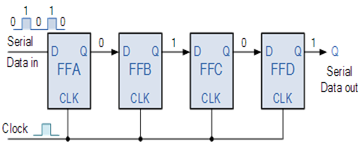
§ Serial-in to Parallel-out (SIPO) - the
register is loaded with serial data, one bit at a time, with the stored data
being available at the output in parallel form.
4-bit
Serial-in to Parallel-out Shift Register

§ Serial-in to Serial-out (SISO) - the
data is shifted serially “IN” and “OUT” of the register, one bit at a time in
either a left or right direction under clock control.
§
§ Parallel-in to Serial-out (PISO) - the
parallel data is loaded into the register simultaneously and is shifted out of
the register serially one bit at a time under clock control.

§ Parallel-in to Parallel-out (PIPO) - the
parallel data is loaded simultaneously into the register, and transferred
together to their respective outputs by the same clock pulse.

2*4 decoder desing using gate [BUET M.SC Admission -2015]

4 bit Parallel Adder which will work for 4 bit
Subtractor too [Electricity Generation Company of Bangladesbh(EGCB)-2018]
The operations of both addition and subtraction can be performed by a one common binary adder. Such binary circuit can be designed by adding an Ex-OR gate with each full adder as shown in below figure. The figure below shows the 4 bit parallel binary adder/subtractor which has two 4 bit inputs as A3A2A1A0 and B3B2B1B0.
The mode input control line M is connected with carry input of the least significant bit of the full adder. This control line decides the type of operation, whether addition or subtraction.

When M= 1, the circuit is a subtractor and when M=0, the circuit becomes adder. The Ex-OR gate consists of two inputs to which one is connected to the B and other to input M. When M = 0, B Ex-OR of 0 produce B. Then full adders add the B with A with carry input zero and hence an addition operation is performed.
When M = 1, B Ex-OR of 0 produce B complement and also carry input is 1. Hence the complemented B inputs are added to A and 1 is added through the input carry, nothing but a 2’s complement operation. Therefore, the subtraction operation is performed.
(a)
f(A,B,C,D,E)= ∑ (0,1,2,8,9,15,17,21,24,25,27,31). Minimize
the function fusing Q-M method. Find essential prime implicants and prime
implicants. [BUET DLD 2017]
(b)Design a negative logic 4 bit parity checker and generator. [BUET DLD 2017]
Parity generator and
checker
A parity generator is a combinational logic circuit that generates the parity bit in the transmitter. On the other hand, a circuit that checks the parity in the receiver is called parity checker. A combined circuit or devices of parity generators and parity checkers are commonly used in digital systems to detect the single bit errors in the transmitted data word.
The sum of the data bits and parity bits can be even or odd . In even parity, the added parity bit will make the total number of 1s an even amount whereas in odd parity the added parity bit will make the total number of 1s odd amount.
The basic principle involved in the implementation of parity circuits is that sum of odd number of 1s is always 1 and sum of even number of 1s is always zero. Such error detecting and correction can be implemented by using Ex-OR gates (since Ex-OR gate produce zero output when there are even number of inputs).
To produce two bits sum, one Ex-OR gate is sufficient whereas for adding three bits two Ex-OR gates are required as shown in below figure.

Parity Generator
It is combinational circuit that accepts an n-1 bit stream data and generates the additional bit that is to be transmitted with the bit stream. This additional or extra bit is termed as a parity bit.
In even parity bit scheme, the parity bit is ‘0’ if there are even number of 1s in the data stream and the parity bit is ‘1’ if there are odd number of 1s in the data stream.
In odd parity bit scheme, the parity bit is ‘1’ if there are even number of 1s in the data stream and the parity bit is ‘0’ if there are odd number of 1s in the data stream. Let us discuss both even and odd parity generators.
Even Parity Generator
Let us assume that a 3-bit message is to be transmitted with an even parity bit. Let the three inputs A, B and C are applied to the circuits and output bit is the parity bit P. The total number of 1s must be even, to generate the even parity bit P.
The figure below shows the truth table of even parity generator in which 1 is placed as parity bit in order to make all 1s as even when the number of 1s in the truth table is odd.

The K-map simplification for 3-bit message even parity
generator is

From the above truth table, the simplified expression
of the parity bit can be written as

Odd Parity Generator
Let us consider that the 3-bit data is to be transmitted with an odd parity bit. The three inputs are A, B and C and P is the output parity bit. The total number of bits must be odd in order to generate the odd parity bit.
In the given truth table below, 1 is placed in the parity bit in order to make the total number of bits odd when the total number of 1s in the truth table is even.

The truth table of the odd parity generator can be
simplified by using K-map as

The output parity bit expression for this generator circuit is obtained as
P = A ⊕ B Ex-NOR C
The above Boolean expression can be implemented by using one Ex-OR gate and one Ex-NOR gate in order to design a 3-bit odd parity generator.
The logic circuit of this generator is shown in below figure , in which . two inputs are applied at one Ex-OR gate, and this Ex-OR output and third input is applied to the Ex-NOR gate , to produce the odd parity bit. It is also possible to design this circuit by using two Ex-OR gates and one NOT gate.

Even Parity Checker
Consider that three input message along with even parity bit is generated at the transmitting end. These 4 bits are applied as input to the parity checker circuit which checks the possibility of error on the data. Since the data is transmitted with even parity, four bits received at circuit must have an even number of 1s.
If any error occurs, the received message consists of odd number of 1s. The output of the parity checker is denoted by PEC (parity error check).
The below table shows the truth table for the even parity checker in which PEC = 1 if the error occurs, i.e., the four bits received have odd number of 1s and PEC = 0 if no error occurs, i.e., if the 4-bit message has even number of 1s.

The above truth table can be simplified using K-map as shown below.


The above logic expression for the even parity checker
can be implemented by using three Ex-OR gates as shown in figure. If the
received message consists of five bits, then one more Ex-OR gate is required
for the even parity checking.

Using NOR gate solve p^ (q v r) ^ ((P^q)-> r). [BUET DLD 2017]
What
is the difference between r's and (r-1)'s complement? (r is the base) [BUET DLD
2017]
Finding the r's and (r-1)'s complement
Here we are going to learn how to
convert a number to its r's and (r-1)'s complement.
Method:
Let 'N' is a number and r is its base
where r>1 and in N, 'n' is the number of digits before its decimal
point then we can write
r's complement of number = r^n-N
EX.
N = (23)10
here r = 10
n = 2 and
N = 23
hence we can write the 10's complement
of this number as 10^2 - 23 = 77.
hence we can say that 10's comp of 23 is
77.
Although this method is good enough to
solve any problem regarding to this concept, but we will follow different
method for finding r's and r-1's complement.
Easy Method:
Let we have to find again the 10's comp
of 23 then this method tells us to divide 3 from 10 and 2 from 9 (i.e 10-9).
which gives us a result of 77.
9
10
- 2
3
7
7
i.e the generalized form of
writing a r's comp of a number 'abc' which is in r base, we can write.
(r-1)
(r-1) r
- a
b c
this difference gives us the r's comp of
that number.
i.e we can find r's complement of a
number by subtracting its right most digit by r and all digits by r-1.
Finding (r-1)'s
complement:
We can do this easily
by subtracting all the digits of that number from (r-1) where r is the
base of that number.
EXAMPLES:
Find the 10's and 9's complement of
(348)10.
ans:
9 9 10
- 3 4 8
6 5
2 here 652 is 10's comp of 348
9's comp
9 9 9
- 3 4 8
6 5
1 here 651 is 9's comp of 348
from this method you can find the r's
and (r-1)'s complement of any number with base r.
if any questions DO COMMENTS..
A
Half Adder Circuit
A half adder is a logical circuit that performs an addition operation on two binary digits. The half adder produces a sum and a carry value which are both binary digits.
Half
Adder Truth Table with Carry-Out
|
Symbol |
Truth
Table |
|||
 |
B |
A |
SUM |
CARRY |
|
0 |
0 |
0 |
0 |
|
|
0 |
1 |
1 |
0 |
|
|
1 |
0 |
1 |
0 |
|
|
1 |
1 |
0 |
1 |
|
From the truth table of the half adder we can see that the SUM (S) output is the result of the Exclusive-OR gate and the Carry-out (Cout) is the result of the AND gate. Then the Boolean expression for a half adder is as follows.
For the SUM bit:
SUM = A XOR B = A ⊕ B
For the CARRY bit:
CARRY = A AND B = A.B
One major disadvantage of the Half Adder circuit when used as a binary adder, is that there is no provision for a “Carry-in” from the previous circuit when adding together multiple data bits.
For example, suppose we want to add together two 8-bit bytes of data, any resulting carry bit would need to be able to “ripple” or move across the bit patterns starting from the least significant bit (LSB). The most complicated operation the half adder can do is “1 + 1” but as the half adder has no carry input the resultant added value would be incorrect. One simple way to overcome this problem is to use a Full Adder type binary adder circuit.
A
Full Adder Circuit
The main difference between the Full Adder and the previous Half Adder is that a full adder has three inputs. The same two single bit data inputs A and B as before plus an additional Carry-in (C-in) input to receive the carry from a previous stage as shown below.
Full
Adder Block Diagram

Then the full adder is a logical circuit that performs an addition operation on three binary digits and just like the half adder, it also generates a carry out to the next addition column. Then a Carry-in is a possible carry from a less significant digit, while a Carry-out represents a carry to a more significant digit.
In many ways, the full adder can be thought of as two half adders connected together, with the first half adder passing its carry to the second half adder as shown.
Full
Adder Logic Diagram

As the full adder circuit above is basically two half adders connected together, the truth table for the full adder includes an additional column to take into account the Carry-in, CIN input as well as the summed output, S and the Carry-out, COUT bit.
Full
Adder Truth Table with Carry
|
Symbol |
Truth
Table |
||||
 |
C-in |
B |
A |
S |
Ca |
|
0 |
0 |
0 |
0 |
0 |
|
|
0 |
0 |
1 |
1 |
0 |
|
|
0 |
1 |
0 |
1 |
0 |
|
|
0 |
1 |
1 |
0 |
1 |
|
|
1 |
0 |
0 |
1 |
0 |
|
|
1 |
0 |
1 |
0 |
1 |
|
|
1 |
1 |
0 |
0 |
1 |
|
|
1 |
1 |
1 |
1 |
1 |
|
Then the Boolean expression for a full adder is as follows.
For the SUM (S) bit:
SUM = (A XOR B) XOR Cin = (A ⊕ B) ⊕ Cin
For the CARRY-OUT (Cout) bit:
CARRY-OUT = A AND B OR Cin(A XOR B) = A.B + Cin(A ⊕ B)
An
n-bit Binary Adder
We have seen above that single 1-bit binary adders can be constructed from basic logic gates. But what if we wanted to add together two n-bit numbers, then n number of 1-bit full adders need to be connected or “cascaded” together to produce what is known as a Ripple Carry Adder.
A “ripple carry adder” is simply “n“, 1-bit full adders cascaded together with each full adder representing a single weighted column in a long binary addition. It is called a ripple carry adder because the carry signals produce a “ripple” effect through the binary adder from right to left, (LSB to MSB).
For example, suppose we want to “add” together two 4-bit numbers, the two outputs of the first full adder will provide the first place digit sum (S) of the addition plus a carry-out bit that acts as the carry-in digit of the next binary adder.
The second binary adder in the chain also produces a summed output (the 2nd bit) plus another carry-out bit and we can keep adding more full adders to the combination to add larger numbers, linking the carry bit output from the first full binary adder to the next full adder, and so forth. An example of a 4-bit adder is given below.
A
4-bit Ripple Carry Adder

One main disadvantage of “cascading” together 1-bit binary adders to add large binary numbers is that if inputs A and B change, the sum at its output will not be valid until any carry-input has “rippled” through every full adder in the chain because the MSB (most significant bit) of the sum has to wait for any changes from the carry input of the LSB (less significant bit). Consequently, there will be a finite delay before the output of the adder responds to any change in its inputs resulting in a accumulated delay.
When the size of the bits being added is not too large for example, 4 or 8 bits, or the summing speed of the adder is not important, this delay may not be important. However, when the size of the bits is larger for example 32 or 64 bits used in multi-bit adders, or summation is required at a very high clock speed, this delay may become prohibitively large with the addition processes not being completed correctly within one clock cycle.
This unwanted delay time is called Propagation delay. Also another problem called “overflow” occurs when an n-bit adder adds two parallel numbers together whose sum is greater than or equal to 2n
One solution is to generate the carry-input signals directly from the A and Binputs rather than using the ripple arrangement above. This then produces another type of binary adder circuit called a Carry Look Ahead Binary Adder where the speed of the parallel adder can be greatly improved using carry-look ahead logic.
For a carry look-ahead adder circuit what advantage do we get if we use it
instead of a 4 bit simple full adder? For "not" gate with 2 ns
propagation delay and other basic gates with 4 ns propagation delay what will
be the total propagation delay? [BUET DLD 2017]
Carry look-ahead adder
In case of
parallel adders, the binary addition of two numbers is initiated when all the
bits of the augend and the addend must be available at the same time to perform
the computation. In a parallel adder circuit, the carry output of each full
adder stage is connected to the carry input of the next higher-order stage,
hence it is also called as ripple carry type adder.
In such
adder circuits, it is not possible to produce the sum and carry outputs of any
stage until the input carry occurs. So there will be a considerable time delay
in the addition process , which is known as , carry propagation delay. In any
combinational circuit , signal must propagate through the gates before the
correct output sum is available in the output terminals.

Consider
the above figure, in which the sum S4 is produced by the corresponding full
adder as soon as the input signals are applied to it. But the carry input C4 is
not available on its final steady state value until carry c3 is available at its
steady state value. Similarly C3 depends on C2 and C2 on C1. Therefore, carry
must propagate to all the stages in order that output S4 and carry C5 settle
their final steady-state value.
The
propagation time is equal to the propagation delay of the typical gate times
the number of gate levels in the circuit. For example, if each full adder stage
has a propagation delay of 20n seconds, then S4 will reach its final correct
value after 80n (20 × 4) seconds. If we extend the number of stages for adding
more number of bits then this situation becomes much worse.
So the
speed at which the number of bits added in the parallel adder depends on the
carry propagation time. However, signals must be propagated through the gates
at a given enough time to produce the correct or desired output.
The
following are the methods to get the high speed in the parallel adder to
produce the binary addition.
1.
By employing faster gates with
reduced delays, we can reduce the propagation delay. But there will be a
capability limit for every physical logic gate.
2.
Another way is to increase the
circuit complexity in order to reduce the carry delay time. There are several
methods available to speeding up the parallel adder, one commonly used method
employs the principle of look ahead-carry addition by eliminating inter stage
carry logic.
Carry-Lookahead Adder
A carry-Lookahead adder is a fast parallel adder as it reduces the propagation delay by more complex hardware, hence it is costlier. In this design, the carry logic over fixed groups of bits of the adder is reduced to two-level logic, which is nothing but a transformation of the ripple carry design.
This method makes use of logic gates so as to look at the lower order bits of the augend and addend to see whether a higher order carry is to be generated or not. Let us discuss in detail.


Consider the full adder circuit shown above with corresponding truth table. If we define two variables as carry generate Gi and carry propagate Pi then,
Pi = Ai ⊕ Bi
Gi = Ai Bi
The sum output and carry output can be expressed as
Si = Pi ⊕ Ci
C i +1 = Gi + Pi Ci
Where Gi is a carry generate which produces the carry when both Ai, Bi are one regardless of the input carry. Pi is a carry propagate and it is associate with the propagation of carry from Ci to Ci +1.
The carry output Boolean function of each stage in a 4 stage carry-Lookahead adder can be expressed as
C1 = G0 + P0 Cin
C2 = G1 + P1 C1
= G1 + P1 G0 + P1 P0 Cin
C3 = G2 + P2 C2
= G2 + P2 G1+ P2 P1 G0 + P2 P1 P0 Cin
C4 = G3 + P3 C3
= G3 + P3 G2+ P3 P2 G1 + P3 P2 P1 G0 + P3 P2 P1 P0 Cin
From the above Boolean equations we can observe that C4 does not have to wait for C3 and C2 to propagate but actually C4 is propagated at the same time as C3 and C2. Since the Boolean expression for each carry output is the sum of products so these can be implemented with one level of AND gates followed by an OR gate.
The implementation of three Boolean functions for each carry output (C2, C3 and C4) for a carry-Lookahead carry generator shown in below figure.

Therefore, a 4 bit parallel adder can be implemented with the carry-Lookahead scheme to increase the speed of binary addition as shown in below figure. In this, two Ex-OR gates are required by each sum output. The first Ex-OR gate generates Pi variable output and the AND gate generates Gi variable.
(b) Using only 2 to 4 line decoder solve a function f(A,B,C,D)= ∏ (3,5,9,15,12,4,1) 2x4 line decoder has
active low enable and outputs are active low. (if gates are required then use
the minimum No. of gates) [BUET DLD 2017]
Decoder/Multiplexer
combining a. Construct a 5-to-32 decoder using only 2-to-4 decoders and 3-to-8
decoders (with enable). b. Design a 32-to-1 multiplexer using only 8-to-1
multiplexer. Use block diagram for the components.
We
are going to make 5-to-32 decoder like the one shown below:

We
need four 3-to-8 decoder for the last stage and one 2-to-4 decoder for
selecting each of them at the first stage:

(c) How can be a decoder used as a demultiplexer? Explain with an example. [BUET
DLD 2017]
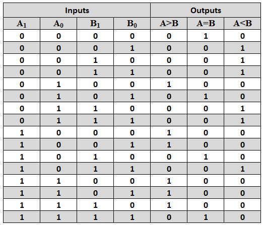
(d) Design and explain a 2 bit magnitude comparator[BUET DLD 2017]
2-Bit Comparator
A 2-bit comparator compares two binary numbers, each of two bits and produces their relation such as one number is equal or greater than or less than the other. The figure below shows the block diagram of a two-bit comparator which has four inputs and three outputs.
The first number A is designated as A = A1A0 and the second number is designated as B = B1B0. This comparator produces three outputs as G (G = 1 if A>B), E (E = 1, if A = B) and L (L = 1 if A<B).

The truth
table of this comparator is shown below which depicting various input and
output states.

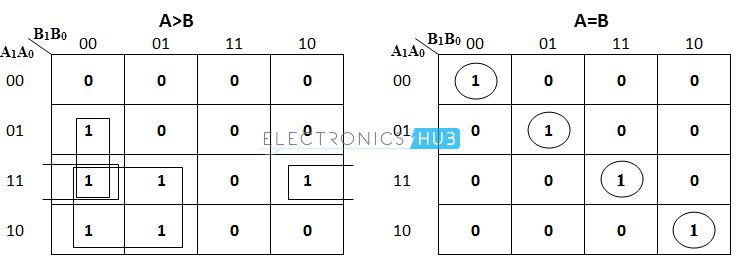
The k-map
simplification for the above truth table is as follows.

From the above k-map simplification, each output can be
expressed as

Q. Design an one-input, one-output serial 2's complementer using D
flip-flops. The
circuit accepts a string of bits from the input and generates the 2's
complement at the
output. The circuit can be reset asynchronously to start and end the operation.
The design
must include [BUET DLD
2016]
(i) State diagram
(ii) State table
(iii) Simplified logic equations
(iv) Logic diagram
(c) Draw the block diagram of Mealy and Moore state machines. [BUET DLD 2016]
The most general model of a
sequential circuit has inputs, outputs, and internal states. It is customary to
distinguish between two models of sequential circuits: the Mealy model and the
Moore model. They differ only in the way the output is generated. In the Mealy
model, the output is a function of both the present state and the input. In the
Moore model, the output is a function of only the present state.

A circuit may have both types of
outputs. The two models of a sequential circuit are commonly referred to as a
finite state machine, abbreviated FSM. The Mealy model of a sequential circuit
is referred to as a Mealy FSM or Mealy machine. The Moore model is referred to
as a Moore FSM or Moore machine.

The above circuit is an example of
mealy machine. Output y is a function of both input x and the present state of
A and B . The corresponding state diagram given below shows both the input and
output values, separated by a slash along the directed lines between the
states.

An example of a Moore model is given
below.

Here, the output is a function of
the present state only. The corresponding state diagram is

It has only inputs marked along the
directed lines. The outputs are the flip-flop states marked inside the circles.
In a Moore model, the outputs of the
sequential circuit are synchronized with the clock, because they depend only on
flip-flop outputs that are synchronized with the clock. In a Mealy model, the
outputs may change if the inputs change during the clock cycle. Moreover, the
outputs may have momentary false values because of the delay encountered from
the time that the inputs change and the time that the flip-flop outputs change.
In order to synchronize a Mealy-type circuit, the inputs of the sequential
circuit must be synchronized with the clock and the outputs must be sampled
immediately before the clock edge. The inputs are changed at the inactive edge
of the clock to ensure that the inputs to the flip-flops stabilize before the
active edge of the clock occurs. Thus, the output of the Mealy machine is the
value that is present immediately before the active edge of the clock.
(a) Write the excitation table for a SR latch constructed with NOR gates. [BUET DLD 2016]
Unclocked S R Flip-Flop
Using NOR Gate
SR flip flop can also be designed by cross coupling of two NOR gates. It is an active high input SR flip – flop. The circuit of SR flip – flop using NOR gates is shown in below figure.

The operation is same as that of NOR SR Latch.
Working
Case 1:
When both the SET and RESET inputs are low, then the output remains in previous state i.e. it holds the previous data
Case 2:
When SET input is low and RESET input is high, then the flip flop will be in RESET state. Because the high input of NOR gate with R input drives the other NOR gate with 0, as its output is 0. So both the inputs of the NOR gate with S input are 0. This will cause the output of the flip – flop to settle in RESET state.
Case 3:
When SET input is high and RESET input is low, then the flip flop will be in SET state. Because the low input of NOR gate with S input drives the other NOR gate with 1, as its output is 1. So both the inputs of the NOR gate with R input are 1. This will cause the output of the flip flop to settle in SET state.
Case 4:
When
both the SET and RESET inputs are high, then the flip flop will be undefined
state. Because the high inputs of S and R, violates the rule of flip flop that
the outputs should complement to each other. So the flip flop is in undefined
state (or forbidden state).
The table below summarizes above explained working of SR Flip Flop designed
with the help of a NOR gate.

Even though simple SR flip – flops and simple SR latches are same, both the terms are used in their respective contexts.
The problem with simple SR flip – flops is that they are level sensitive to the control signal (although not shown in figure) which makes them a transparent device. In order to avoid this, Gated or Clocked SR flip – flops are introduced (whenever the term SR flip – flop is used, it usually refers to clocked SR flip – flop). Clock signal makes the device edge sensitive (and hence no transparency).
(a)
Prove the following Boolean algebra theorem: (x + y )(x’+ z )(y
+ z) = (x + y )(x’ + z). [BUET DLD 2016]
(b) How many distinct Boolean functions are there of n Boolean
variables? [BUET DLD 2016]
(c) Show that NAND gate is a universal logic gate. Also show that NAND
operation doesn't follow associative law. [BUET DLD 2016]
The
“Universal” NAND Gate
The Logic NAND Gate is generally classed as a “Universal” gate because it is one of the most commonly used logic gate types. NAND gates can also be used to produce any other type of logic gate function, and in practice the NAND gate forms the basis of most practical logic circuits.
By connecting them together in various combinations the three basic gate types of AND, OR and NOT function can be formed using only NAND gates, for example.
Various
Logic Gates using only NAND Gates

As well as the three common types above, Exclusive-OR, Exclusive-NORand standard NOR gates can be formed using just individual NAND gates.
Nope. Say you have 3 variables, A and B and C, which can
either be true (1) or false (0). NAND is “not and,” so:
A NAND B
would be the same as
NOT(A AND B).
which is the same as (NOT A) OR (NOT
B).
If you have difficulty remembering
this, just read it aloud and it’ll make sense soon enough.
So A NAND B would only
produce false if both A and B are true.
Here is a a truth table given that A
is true along with the evaluation of (A NAND B) NAND C and the evaluation of A
NAND (B NAND C):


0 মন্তব্যসমূহ